Power and Safety Latching Circuit
Takes various fault sensor inputs and provides latching functionality disabling the EV high voltage system
Controls status indicator lights for safety, communication, and rapid telemetry gathering
Interactive PCB Hardware
Click, drag, and zoom, or tap, two finger drag, and pinch (mobile)
to inspect board routing and component placement
The Objective
The Power and Safety Latching Board is the primary hardware safety barrier for the electric vehicle. Not only is it designed to physically latch and isolate the Battery Management System (BMS), Insulation Monitoring Device (IMD), and Brake System Plausibility Device (BSPD) fault conditions, but also the scope was eventually expanded to include control systems for the car’s high-voltage status indicators as well as execute a startup lamp check sequence. Finally, it was deemed necessary to have an avenue for software from the Vehicle Control Unit (VCU) to shut down the car, and the best interface for software shutdown was on this Latching Board.
System Architecture
The core latching/switching logic relies on Omron G6B-22-14P Normally Open (NO), double-pole relays. The NO configuration satisfies the strict competition rules, while containing two poles allows the safety signal to pass though without interacting with the fault signals. CYTLP127(TP) “Darlington” optocouplers with BJT outputs were used for voltage shifting which provided the necessary current to drive the relay coils. Additionally, TLP291-4 optocouplers transmit the status of each fault sensor signal as well as discrete physical automotive fault locations to our digital datalogging and data acquisition (DAQ) board. Later in the design process, a Normally Closed (NC) relay was added so the VCU can trigger a hardware shutdown with software commands.
To manage the visual safety indicators, 555 timers were introduced to the architecture. One 555 timer allows one of the high-voltage status indicators to blink at 3.24Hz, which is in the rules specified frequency range of 2-5Hz. The feedback components added to this circuit were chosen to make it easy to hotswap and change the frequency in the event of a rules change. Another 555 timer was used for the lamp check upon powering the car. As the car powers up, multiple dash and LED indicators around the car must turn on for a set duration to verify the indicators are working. This lamp check sequence also resets and proceeds to allow the Latching Circuit to turn on and function shortly after the car turns on.
Design Rationale & Challenges
One of the biggest challenges was that this is the first generation of this board, and with that, there are still many unknowns from both a competition side, and our own architecture side. Each fault indicator might have different levels of voltage and current for example. This board is optimized for high-impedance, open-drain faults, with many Do Not Populate (DNP) pads for future proofing and quick configuration if for example it turns out a signal is low-side signaling instead of the expected high-side. Furthermore, back-current protection diodes prevent relay coil inductive kickback from frying the sensor boards, or even the board traces and other passive components. All this is maintained while the LEDs placed on the board provide immediate visual diagnostics.
Another challenge was integrating all the scope creep additions to the board. Each addition added its own diode ORing logic whether that’s different methods of reset or that’s adding the lamp check functionality onto the indicator functionality. MOSFET ideal ORing is more stable and reliable, but the board would’ve gotten way too complex for the scope, as well as add logic that’s harder to debug and introduce more places for error. The simpler diode ORing worked by adding the appropriate pull-down networks to ensure the MOSFET gates did not remain floating thus locking conduction when we don’t want conduction.
Outcome & Validation
The board successfully isolates the high-voltage system upon receiving the fault signals and sends the faults to the DAQ board while maintaining isolation as verified with the “fault injection” switches. The DNP footprints allowed for easy adapting and evolving of architecture and hardware specifications. The 555 timers allowed for consistent, easily changeable timer logic for the boot sequence and indicators which were easily verified with hand timers or an oscilloscope. Finally the diode ORing maintained the simplicity without sacrificing reliability.
Technical Specifications
- Core Components: Relays, Optocouplers
- Architecture: Latching and Control Circuit
- Interfaces: Fault Input Signals, Status Indicators
- Tools Used: Altium Designer, JLCPCB, LTspice, SolidWorks
Board Routing
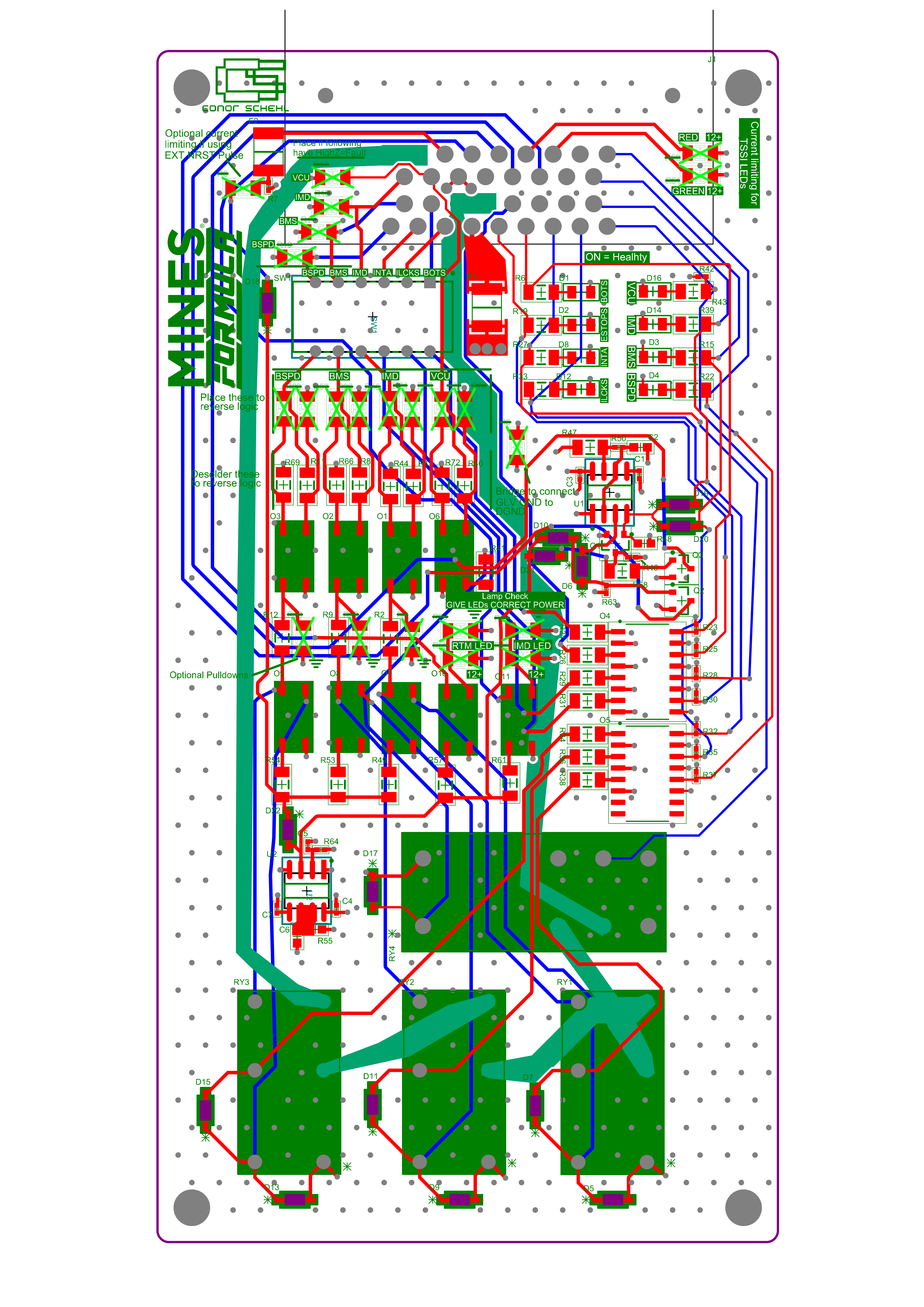
Click to view full resolution
System Architecture
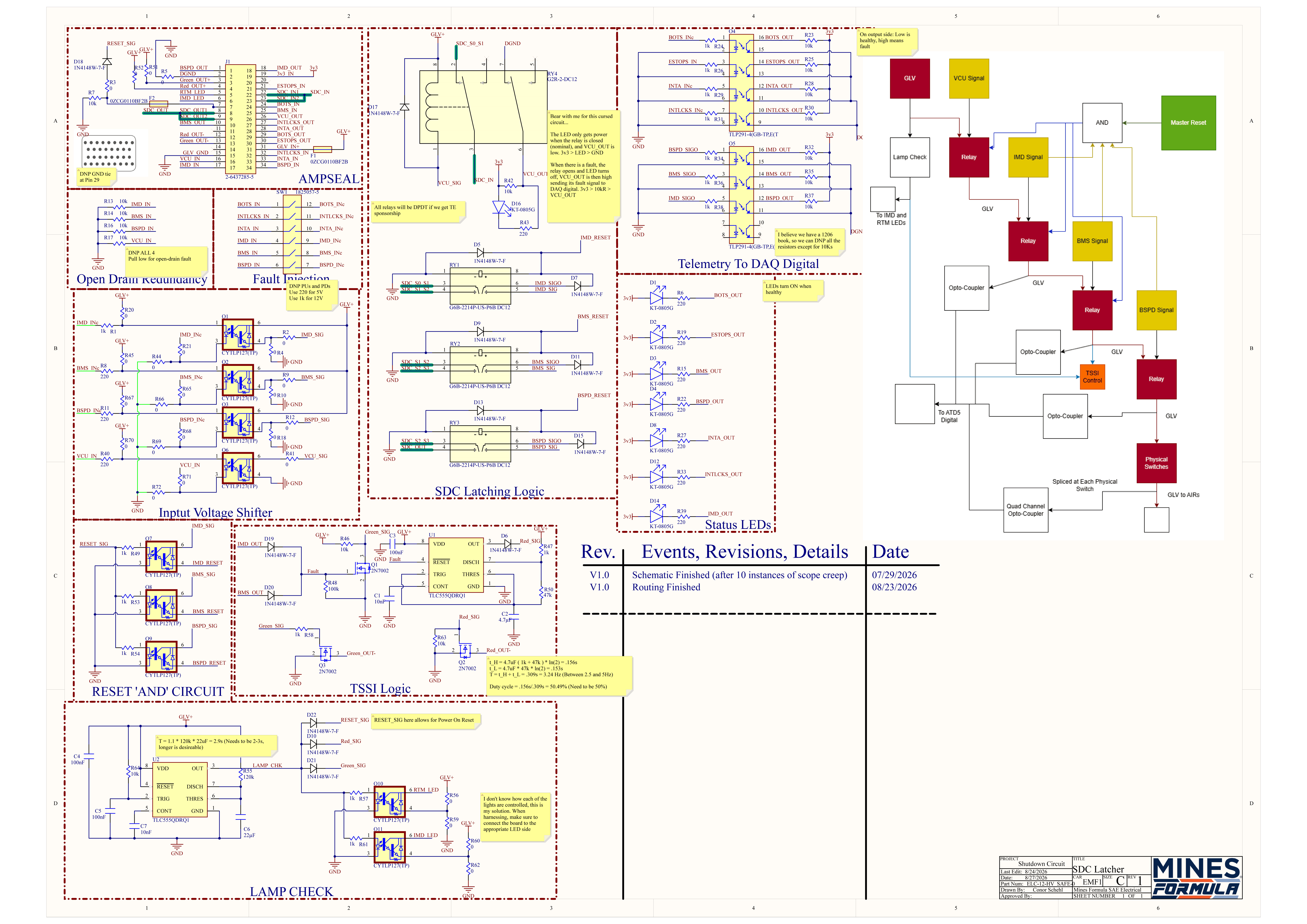
Click to view full resolution